
From GPUs to FPGAs – An Introduction to High-Performance Computing
Introduction
In this post, we look into parallel, as opposed to sequential, computation, specialized hardware, in particular Graphics Processing Units (GPUs) and Field-Programmable Gate Arrays (FPGAs), and High Performance Computing (HPC). This background is essential in the deployment of ML models in high-throughput or resource-constrained contexts.
Parallelism
Traditionally, computer software has been sequential. A computer program was constructed as a series of instructions to be executed one after the other on the Central Processing Unit (CPU) of the computer. Parallel computing [Ref], on the other hand, uses multiple processing elements in order to tackle a problem simultaneously. Many tasks are essentially a repetition of the same calculation a large number of times. So, if these calculations are independent from each other, why wait for each one to finish before proceeding to the next one? The execution can be performed in parallel and thus the routine can be sped up. Historically, parallel computing was used for scientific problems and simulations, such as meteorology. This led to the design of parallel hardware architectures and the development of software needed to program these architectures, as well as HPC [Ref].
Amdahl’s Law
Ideally, doubling the number of processors would result in the halving of the runtime. However, in practice, very few algorithms achieve optimal speedup. The maximum potential speedup is given by Amdahl’s law [Ref]. A task executed on a multicore system can be categorized into two parts: a part that does not benefit from the usage of multiple cores, and a part that does benefit. Assuming that the latter is a fraction \(\tau\) of the task, and that it benefits from an acceleration by a factor \(s\) compared to single core execution then, the maximum speedup is given by:
\[ \text{Speedup}(s) = \frac{1}{1 - \tau + \frac{\tau}{s}} \,. \]
The relationship is illustrated in Fig. 1. Interestingly, this law reveals that increasing the number of processors yields diminishing returns past a certain point. In addition, it demonstrates that the enhancements of the code have to be focused on both the parallelizable and non-parallelizable components. Of course, the simplistic view of computation needed for the derivation of Amdahl’s law neglects various aspects of inter-process communication, synchronization and memory access overheads. A more complete assessment is given by Gustafson’s law [Ref].
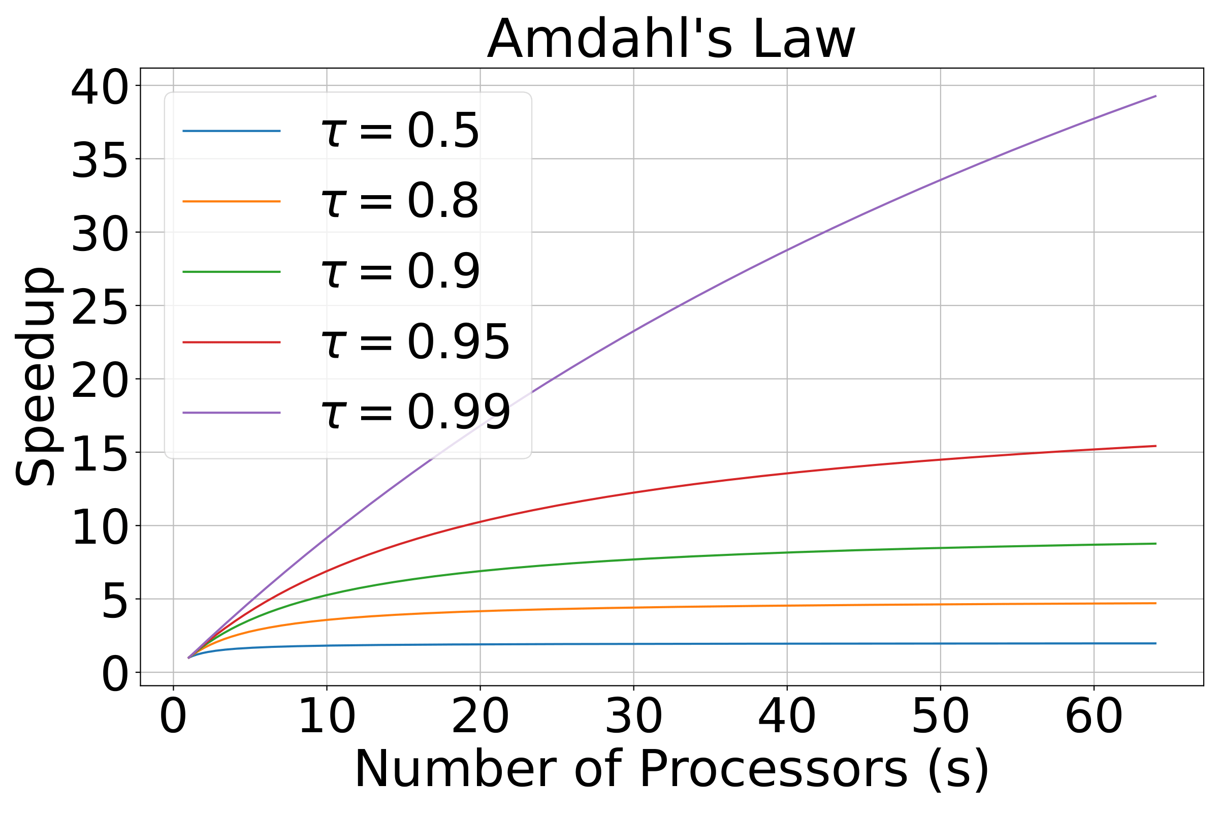
Figure 1: Demonstration of Amdahl’s law for the theoretical maximum speedup of a computational system, as a function of the fraction of the parallelizable code \(\tau\), and the speedup factor \(s\) that the parallelization results in.
The CPU as a Parallel Processor
During the 1980s until the early 2000s, various methods were developed for increasing the computational performance of the CPU. A crucial method was frequency scaling: By increasing the clock frequency of the CPU, more instructions can be executed in the same amount of time. Other methods included the use of reduced instruction sets, out-of-order execution, memory hierarchy or vector processing.
The Dennard scaling law was introduced in 1974 [Ref] and it stated that as transistors get smaller the power consumption of a chip of constant size stays the same even if the number of transistors increases. As transistors became smaller and operating voltages decreased, circuits were able to run at higher frequencies without increasing power consumption. However, this scaling is considered to have broken down around 2006. Dennard scaling overlooked factors like the “leakage current” and the “threshold voltage”, which set a minimum power requirement per transistor. As transistors shrink, these parameters don’t scale proportionally, leading to an increase in power density. This created a so-called “power wall”, as shown in Fig. 2, that practically limited processor frequency to around 4 GHz [Ref], and which eventually led to Intel canceling the Tejas and Jayhawk microprocessors in 2004 [Ref].
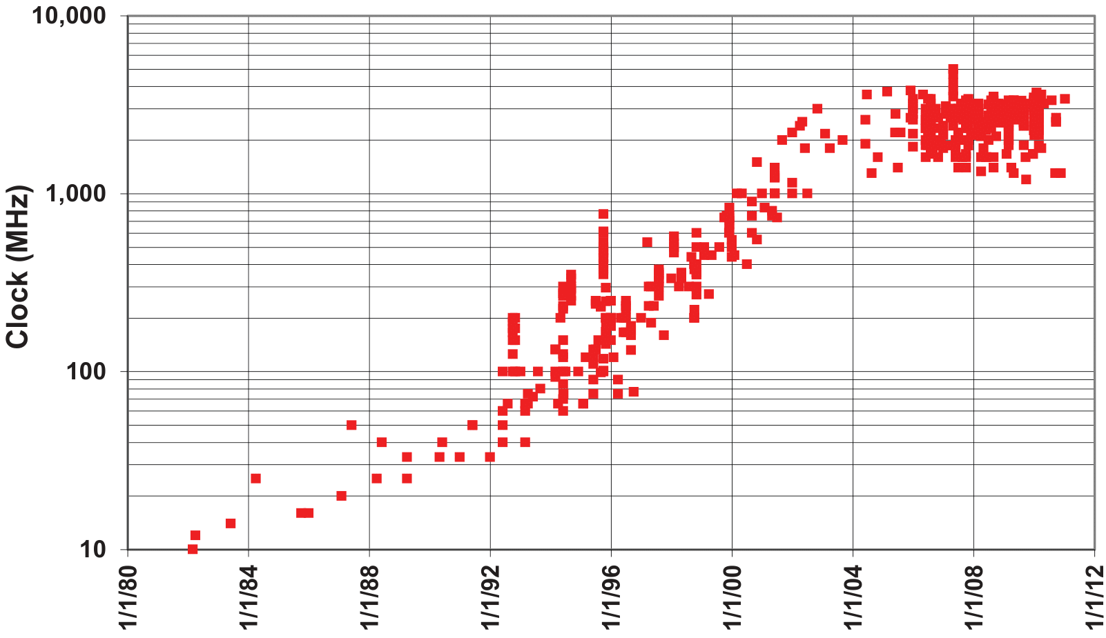
Figure 2: Historical evolution of microprocessor clock rates from 1980 to 2012, illustrating the scaling plateau beginning in 2004. This effect demonstrates the breakdown of Dennard scaling and the so-called “power wall”, limiting further gains through increased frequency due to thermal and energy constraints. Figure from [Ref].
In order to address the problem of power consumption, manufacturers turned to producing power efficient processors that have multiple cores. Each core is independent and can access the same memory concurrently. This design principle brought multi-core processors to the mainstream. By early 2010s, computers by default had multiple cores, while servers had more than ten core processors. By contrast, in early 2020s, some processors had over one hundred cores [Ref]. Moore’s law [Ref], that predicts that the number of transistors in an integrated circuit will double every roughly two years, can be extrapolated to the doubling of the number of cores per processor.
The operating system of the CPU ensures that the different tasks are performed concurrently using the resources of the processor by distributing them across the free cores. However, in order to unlock the full capacity of the processing unit, the code itself has to be designed in a way that leverages the new computational capabilities of multicore architectures [Ref].
Flynn’s Taxonomy
One of the earliest classifications of parallel computers and programs is the so-called Flynn’s taxonomy [Ref]. It categorizes programs based on whether they are operating using a single instruction or multiple instructions, and whether these instructions are executed on one or multiple data.
An entirely sequential program is equivalent to the Single Instruction Stream, Single Data Stream (SISD) classification. When the operation is repeated over multiple data, it corresponds to the Single Instruction Stream, Multiple Data Stream (SIMD) class, a form of data parallelism. On the other hand, when multiple instructions are performed on a single data, a form of dataflow parallelism, the program is classified as Multiple Instruction Stream, Single Data Stream (MISD). While systolic arrays are sometimes put in this category, the class is rather rare in practice. Multiple Instruction Stream, Multiple Data Stream (MIMD) is by far the most common type of modern programs, and is known as control parallelism. The taxonomy is summarized in Fig. 3.
In this context, data dependencies are a crucial aspect of implementing parallel code. If we have a sequence of steps, and each step depends on the result of the previous step then this sequence is not parallelizable since it must be executed in order. However, most algorithms contain opportunities where the execution can be parallelized. Notable examples of this are deep learning algorithms.
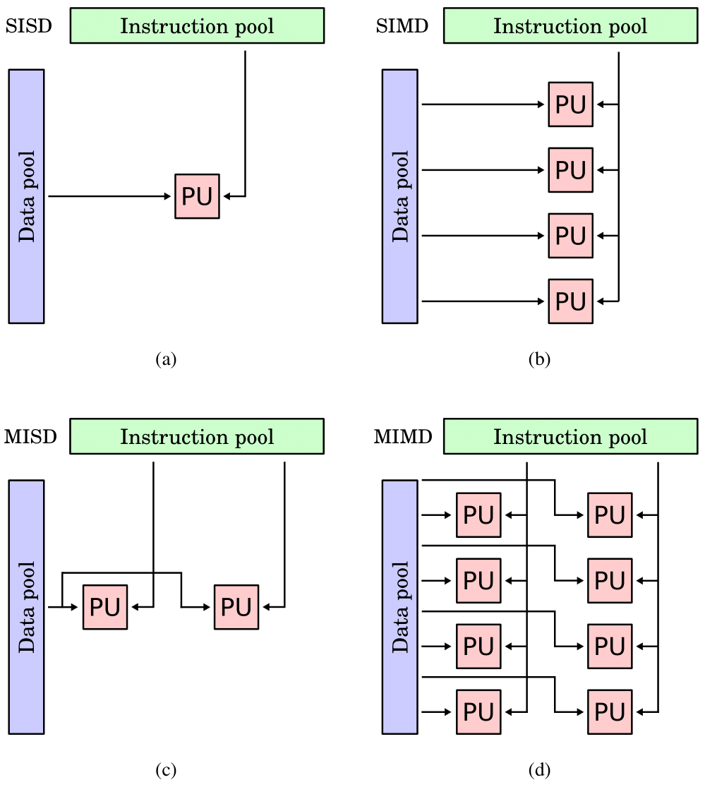
Figure 3: Flynn’s Taxonomy. (a) Single Instruction Stream, Single Data Stream (SISD), (b) Single Instruction Stream, Multiple Data Stream (SIMD), (c) Multiple Instruction Stream, Single Data Stream (MISD), (d) Multiple Instruction Stream, Multiple Data Stream (MIMD). The instruction and data pools are shown, as well as the Processing Units (PUs). Figures from [Ref], [Ref], [Ref] and [Ref].
![[Ref]](https://commons.wikimedia.org/wiki/File:SISD.svg)
![[Ref]](https://commons.wikimedia.org/wiki/File:SIMD.svg)
![[Ref]](https://commons.wikimedia.org/wiki/File:MISD.svg)
![[Ref]](https://commons.wikimedia.org/wiki/File:MIMD.svg)
From Video Games to the GPU Architecture
Early arcade video games used specialized video hardware to handle graphics due to expensive memory units since the 1970s. The first integrated graphics processing unit, NEC’s μPD7220, was the most well known GPU until the mid-1980s. It supported graphics display monitors of \(1024 \times 1024\) resolution, and laid the foundations for the GPU market [Ref].
Early 3D graphics emerged in the 1990s in arcades and consoles and GPUs started integrating 3D functions. The term GPU was coined by Sony in reference to their 32-bit Sony GPU used in the PlayStation 1 video game console, released in 1994 [Ref]. Nvidia and ATI started creating consumer graphics accelerators, leading to the release of GeForce 256. This GPU was marketed as the world’s first GPU capable of performing advanced graphics rendering. These capabilities included tasks such as rasterization, where an image described in a vector graphics format is translated into an array of pixels that best represents this vector description in the available screen granularity. Shading, another essential task for a graphics processor, is the process through which a GPU calculates the appropriate levels of light and color, in order to render a 3D scene more realistically. The first GPU capable of shading was the GeForce 3, used in the Xbox console, competing with the chip used in PlayStation 2.
Nvidia introduced the Compute Unified Device Architecture (CUDA) in 2006, sparking what is now known as General-Purpose Graphics Processing Unit (GPGPU) computing [Ref]. This marked a revolution in computing: previously, GPUs were dedicated chips designed to accelerate 3D rendering tasks for gaming and graphics applications. With CUDA, GPUs became programmable parallel processors equipped with hundreds of processing elements, enabling them to perform a broad range of tasks traditionally tackled using CPUs. This can include scientific computing (simulations, climate, etc.), financial modeling, signal processing, machine learning and deep learning. For the first time, Nvidia provided a dedicated programming model and language for its GPUs, enabling developers to write general-purpose code that could run directly on the GPU—something that was previously not possible with such flexibility and ease.
CUDA is a proprietary language, which led to the need for a standardized parallel programming language that could be used across GPUs from different manufacturers. In response, OpenCL [Ref] was defined by Khronos Group as an open standard. It allows the development of code compatible with both GPU and CPU. This emphasis on portability—the ability to write a single kernel that can run across heterogeneous platforms—made OpenCL the second most popular HPC tool at the time [Ref].
In the 2010s, GPUs were used in consoles such as the PlayStation 4 and the Xbox One [Ref], and on automotive systems, after Nvidia partnered with Audi to power car dashboard displays [Ref]. Nvidia architectures developed further, increasing the number of CUDA cores and further adding the new technology of the so-called tensor cores [Ref]. Tensor cores were designed to bring better performance to deep learning operations. Real-time ray tracing—simulation of reflections, shadows, depth of field, etc.—debuted with Nvidia RTX 20 series in 2018 [Ref].
In 2020s, after the deep learning explosion from 2012 onwards, GPUs are heavily used in the training and inference of large language models, such as the ChatGPT [Ref] chatbot by OpenAI. This surge in interest of dedicated hardware, infrastructure and electricity to support these heavy models has created a booming artificial intelligence ecosystem. It is further fueling a re-evaluation of our electricity needs, infrastructure organization, and the direction of hardware development, while also raising questions about the feasibility of continued scaling.
CUDA Programming Model
Introduced in 2006 by Nvidia [Ref], CUDA is a parallel programming model designed for developing general purpose applications that leverage the parallelization capabilities and architecture of Nvidia GPUs. It can be thought of as an Application Programming Interface (API) that allows software to access the GPU’s virtual instruction set and parallel computation elements for the execution of compute kernels.
The C++ version of CUDA is a language extension of C++ that allows the programmer to define specific parallel functions called kernels, and run code on CPU and GPU using a single language [Ref]. By splitting the code into a host (traditional CPU) and a device (GPU) part, the instructions dictated by the CPU are executed on the GPU. The device code is organized into kernels, and kernels are executed by the threads available on the GPU. Multiple threads execute the same kernel simultaneously, in the so-called Single Instruction, Multiple Threads (SIMT) execution model. SIMT can be thought of as a subcategory of SIMD. In SIMD, a single thread executes an instruction on multiple data. On the other hand, in SIMT, a small group of threads called a warp executes the same instruction on multiple data, but each thread has its own independent program counter, stack and registers, so threads can have divergent execution. This per-thread autonomy gives more flexibility to the SIMT execution model.
Memory Hierarchy
In the CUDA programming model, threads are organized into blocks. In particular, threads that execute the same instruction are grouped into warps and several warps constitute a thread block. Blocks of threads are further organized into grids. These two levels—blocks and grids—correspond to different communication bandwidths and shared memory capacities. Blocks have shared memory that is accessible to all threads in the block, while threads from the different blocks only share the view of the device memory. The model is summarized in Fig. 4.
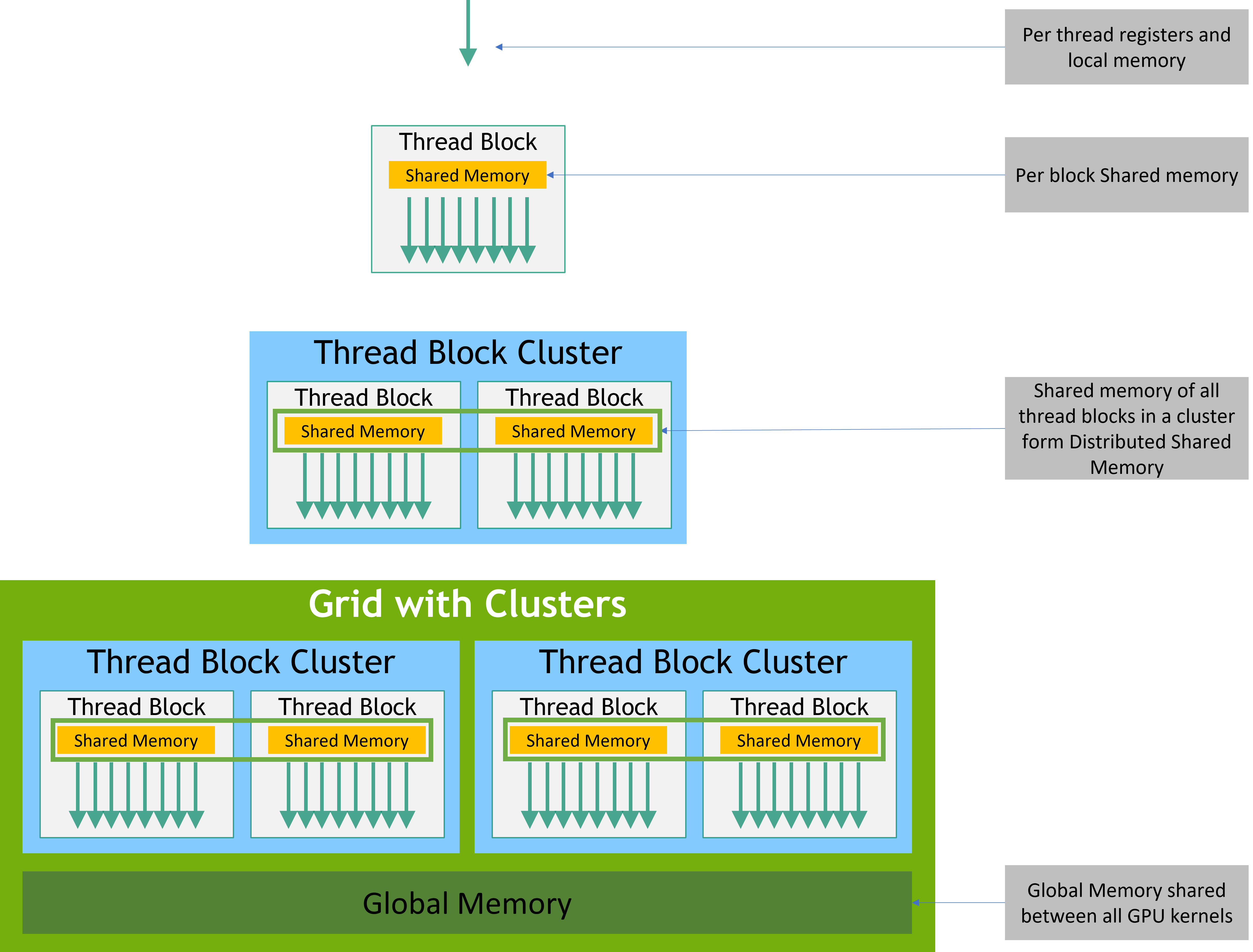
Figure 4: CUDA thread and memory hierarchy. Figure from [Ref].
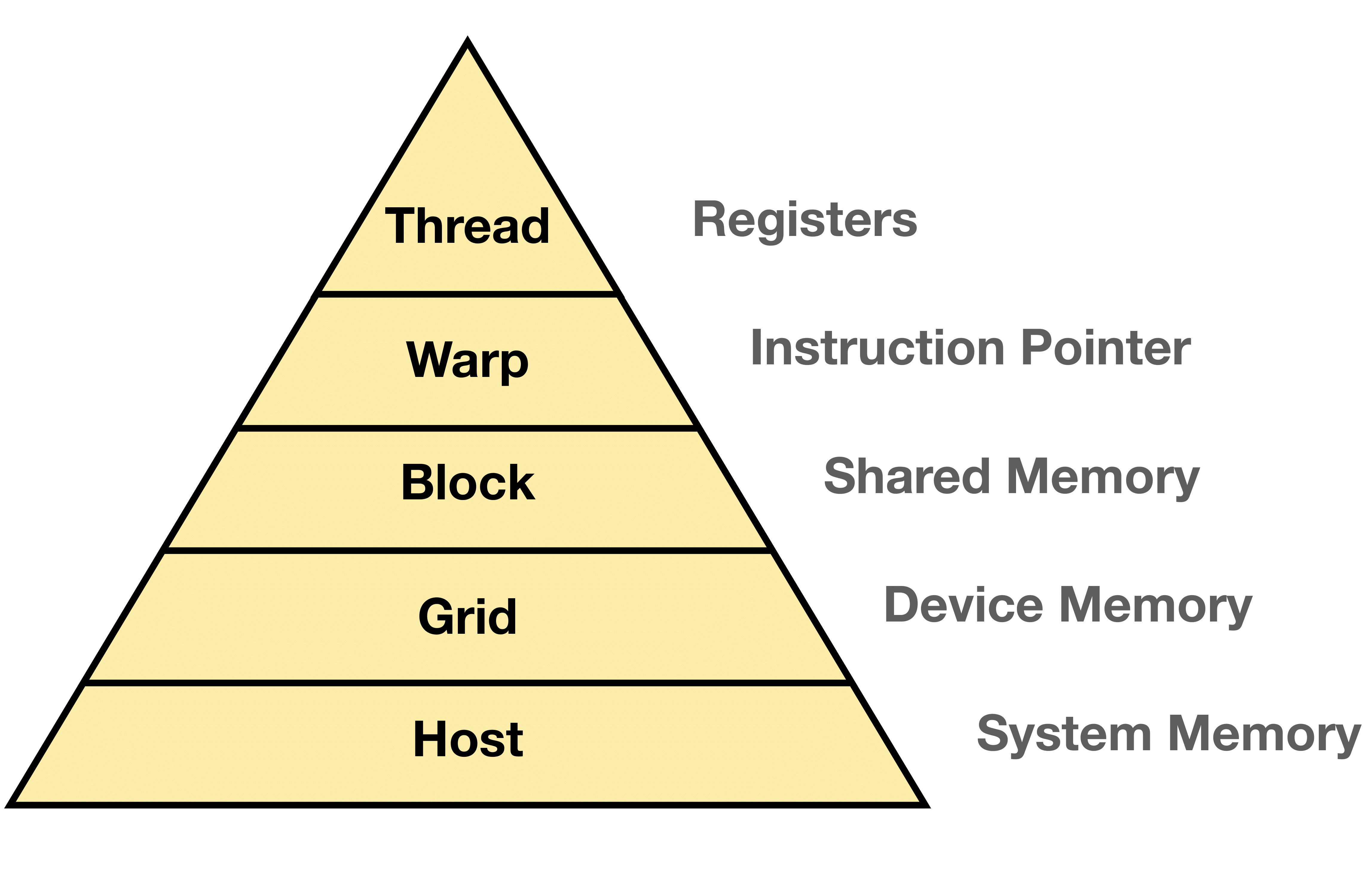
Figure 5: Illustration of the memory hierarchy for a Single Instruction, Multiple Threads (SIMT) program. Inspired by [Ref].
Register memory, is the fastest kind of memory but is of the smallest size, usually around 1 KB per thread. Shared memory, on the other hand, is slower, accessible by all the threads within a block, and is usually on the order of hundreds of kilobytes. The device memory, even slower, is accessible by all the threads of the device and is what is commonly known as Random Access Memory (RAM). As of 2025, most modern GPUs do not go over 80 GB of RAM. Finally, the host RAM is the most costly, in terms of access latency. The memory hierarchy is illustrated in Fig. 5, along with Fig. 4.
Architecture
The GPU delivers significantly higher instruction throughput and memory bandwidth than the CPU, all with similar cost and power range. Various applications take advantage of these enhanced capabilities compared to the CPU, such as GPGPU programming. While FPGAs are also energy-efficient, GPUs offer unmatched programming flexibility.
This difference stems from fundamental design differences. The CPU is optimized to execute a series of operations, by a single thread, at the highest clock frequency possible, and can handle a few dozen concurrent threads. In contrast, GPUs are designed to run thousands of threads in parallel, exploiting data parallelism, but at a lower frequency. However, by trading off individual speed, a much higher overall throughput can be achieved.
To support this level of parallelism, GPUs devote more transistors to data processing rather than to data caching and control logic. This design philosophy is illustrated in Fig. 6, which compares the typical allocation of resources between a CPU and a GPU.
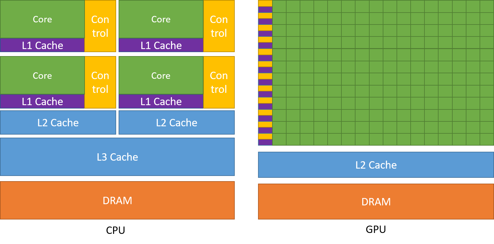
Figure 6: Comparison of the allocation of resources between a CPU and a GPU. Figure from [Ref].
Nvidia’s GPU architecture is an array of the so-called Streaming Multiprocessors (SMs). A multithreaded program is divided into thread blocks that run independently of one another. When a kernel is launched over several blocks, the blocks are distributed across the available SMs for execution. An SM can execute multiple blocks simultaneously. On a GPU with more SMs, the program will be executed automatically in less time than a GPU with fewer multiprocessors. In this way, scaling is automatically guaranteed.
C++ Extension
In the C++ version of CUDA, compute kernels are defined as C++ functions using the __global__ declaration specifier. The launch of the kernel is defined using the CUDA execution configuration syntax <<<K,M>>>(...). In this way, a kernel is launched on K blocks per grid, each with M threads, and is executed in parallel by the active threads. Furthermore, CUDA exposes built-in variables that can be accessed by the developer. In particular, threadIdx gives the identifier of the thread currently executing and blockDim gives the block dimension, i.e., the number of threads in each block—M above. Finally, blockIdx gives the identifier of the block currently in execution. These three variables are 3-component vectors, providing a natural way to invoke computations on vectors, matrices and volumes.
As an example, in Listing 1, an implementation of “Single-precision A*X Plus Y (SAXPY)” [Ref] is presented, a basic function of the Basic Linear Algebra Subroutines (BLAS) library, in CUDA/C++. The saxpy function takes two \(n\)-dimensional input vectors, \(\mathbf{x}\) and \(\mathbf{y}\), as well as a scalar \(a\). It then computes the expression \(a \times (\mathbf{x})_i + (\mathbf{y})_i\), and stores the result in \(\mathbf{y}\). In the host code, we start by moving the prepared data of \(\mathbf{x}\) and \(\mathbf{y}\) from the host to the device. We then invoke the kernel with 4096 blocks, of 256 threads each, for a total of 1048576 active threads (line 21). In this way we launch exactly the number of threads we need to perform the calculation on the number of elements \(N=1\,048\,576\). Each thread is supposed to perform the calculation of each element independently, so in the device code, threads first calculate the index of the element they need to calculate (line 4). After checking that this index does not exceed the length of the vector \(n\) (line 5), they then perform the calculation (line 6). The data are moved from the host to the device and back using API calls (lines 16, 17, 24).
// Device code (kernel definition)
__global__ void saxpy(int n, float a, float *x, float *y)
{
  int i = blockIdx.x*blockDim.x + threadIdx.x;
  if (i < n) {
    y[i] = a*x[i] + y[i];
  }
}

int main(void)
{
  // ...
  int N = 1<<20; // 2^20 = 1048576

  // Copy data from host to device
  cudaMemcpy(x_device, x_host, N*sizeof(float), cudaMemcpyHostToDevice);
  cudaMemcpy(y_device, y_host, N*sizeof(float), cudaMemcpyHostToDevice);

  // Perform SAXPY on 1M elements
  // Invoke kernel with 4096 blocks of 256 threads each
  saxpy<<<4096, 256>>>(N, 2.0f, x_device, y_device);

  // Transfer result back to the host
  cudaMemcpy(y_host, y_device, N*sizeof(float), cudaMemcpyDeviceToHost);

  // ...
}
Listing 1: Saxpy implementation in CUDA C++. Adapted from [Ref].
CUDA threads operate on a physically separate device to the host running the C++ script. The kernel is invoked by the host, but it runs on the device. The execution model is illustrated in Fig. 7.
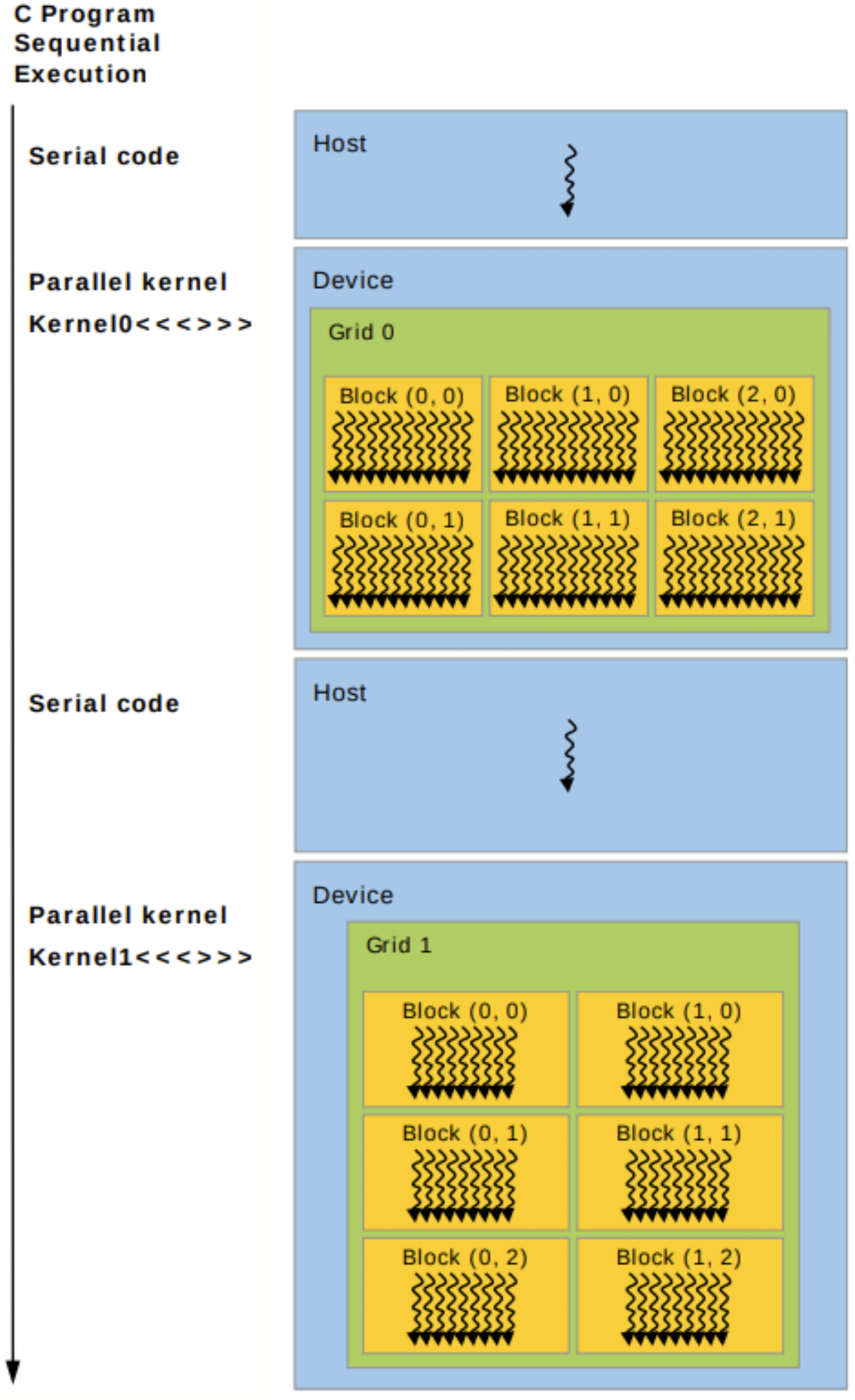
Figure 7: Illustration of heterogeneous programming using the CUDA programming model. Adapted from [Ref].
Programmable Logic
While GPUs are programmable parallel processors designed for general-purpose computing, FPGAs are electronic chips that enable the integration of dedicated parallel architectures. The FPGA sprouted from developments in technology around programmable logic, and in particular from Programmable Read-Only Memory (PROM) and Programmable Logic Devices (PLDs). Both PROMs and PLDs could be programmed outside the factory, i.e., in the field, which explains the “field-programmable” part of the abbreviation [Ref].
Altera, founded in 1983, produced the first erasable programmable ROM circuit in 1984. However, Xilinx delivered the first commercial field-programmable gate array in 1985, the XC2064. Until the mid-1980s, FPGAs were only used in networking and telecommunications. However, by the end of the decade, FPGAs had been adopted across consumer, automotive, and industrial applications [Ref]. With the AI boom around the 2010s, FPGAs are increasingly being used for applications in constrained environments and for prototyping.
FPGAs are extremely versatile due to the fact that they are reconfigurable. This allows developers to test numerous designs after the board has been built. When changes to the design are required, the device is simply restarted and the configuration file, usually called the bitstream, is transferred onto the device.
In particular, FPGAs are crucial for designing Application-Specific Integrated Circuits (ASICs). The manufacture of ASICs is extremely costly, so before a design is decided and put into production, it has to be prototyped. The digital hardware design is then verified and finalized.
Field-Programmable Gate Arrays
The most common FPGA architecture includes an array of Configurable Logic Blocks (CLBs), Input/Output (I/O) cells, and routing channels [Ref], as illustrated in Fig. 8. The CLB typically consists of a Lookup Table (LUT) and a clocked Flip-Flop (FF). An LUT of \(n\)-bit input can encode any Boolean function of \(n\) inputs by simply storing the value of the function for each input, i.e., by storing its truth table. FFs on the other hand, are used to register the value of the output of the logic function and to synchronize the data with the system clock. In this way, by storing the value of a state, sequential logic can be implemented. The routing channels are used to interconnect the logic blocks, and the I/O pads are used for interfacing with external signals. By “configuring” an FPGA, the developer can define the arrangement of these logic gates and their connections, in order to implement a series of operations such as additions, subtractions and logical operations.
FPGAs are often also equipped with Digital Signal Processing (DSP) blocks, responsible for performing more complex operations such as multiplications and divisions. These operations become more and more complex as the bit width of the operands increases. Furthermore, Block RAM (BRAM) is often added on the CLB grid, to enable the storage of large amounts of data inside the FPGA.
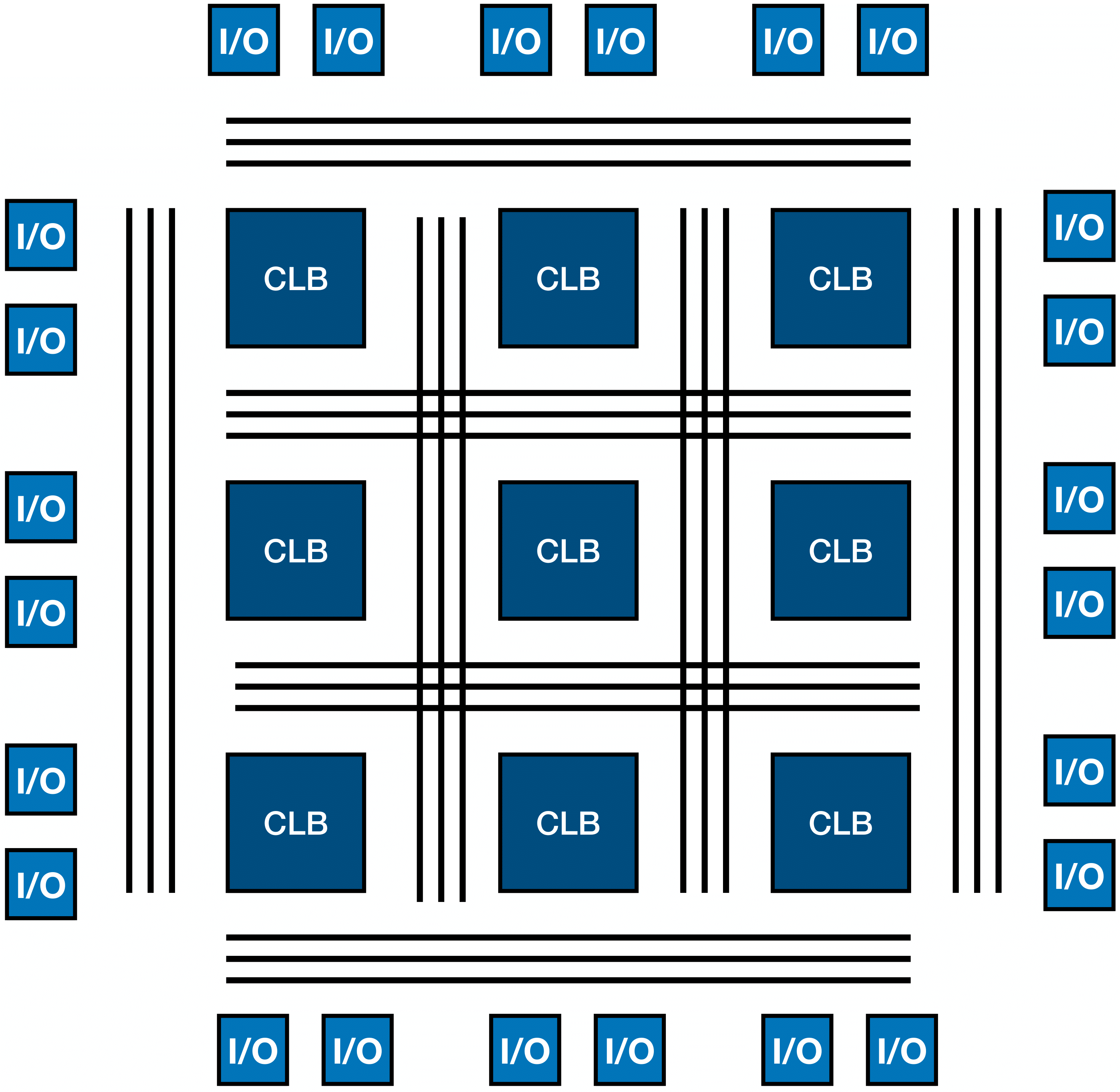
Figure 8: Illustration of the structure of an FPGA, highlighting its three fundamental digital logic components: Configurable Logic Blocks (CLBs), Input/Output (I/O) pads, and routing channels. Inspired by [Ref].
System on a Chip FPGAs
Often, FPGAs are sold as a System on a Chip (SoC). The SoC board is divided into two parts, the Processing System (PS) and the Programmable Logic (PL), as shown in the block diagram in Fig. 9. This type of diagram is a high-level representation showing the main functional components of the FPGA and how these are connected. It is used to understand the internal organization of the chip.
The PS is a traditional CPU, while the PL is the traditional reconfigurable FPGA part. SoCs comprise many execution units. These units communicate by sending data and instructions between them. A very common data bus for SoCs is ARM’s Advanced Microcontroller Bus Architecture (AMBA) standard. Direct memory access controllers transfer data directly between external interfaces and the SoC memory, bypassing the CPU or control unit, which enhances the overall data throughput of the SoC.
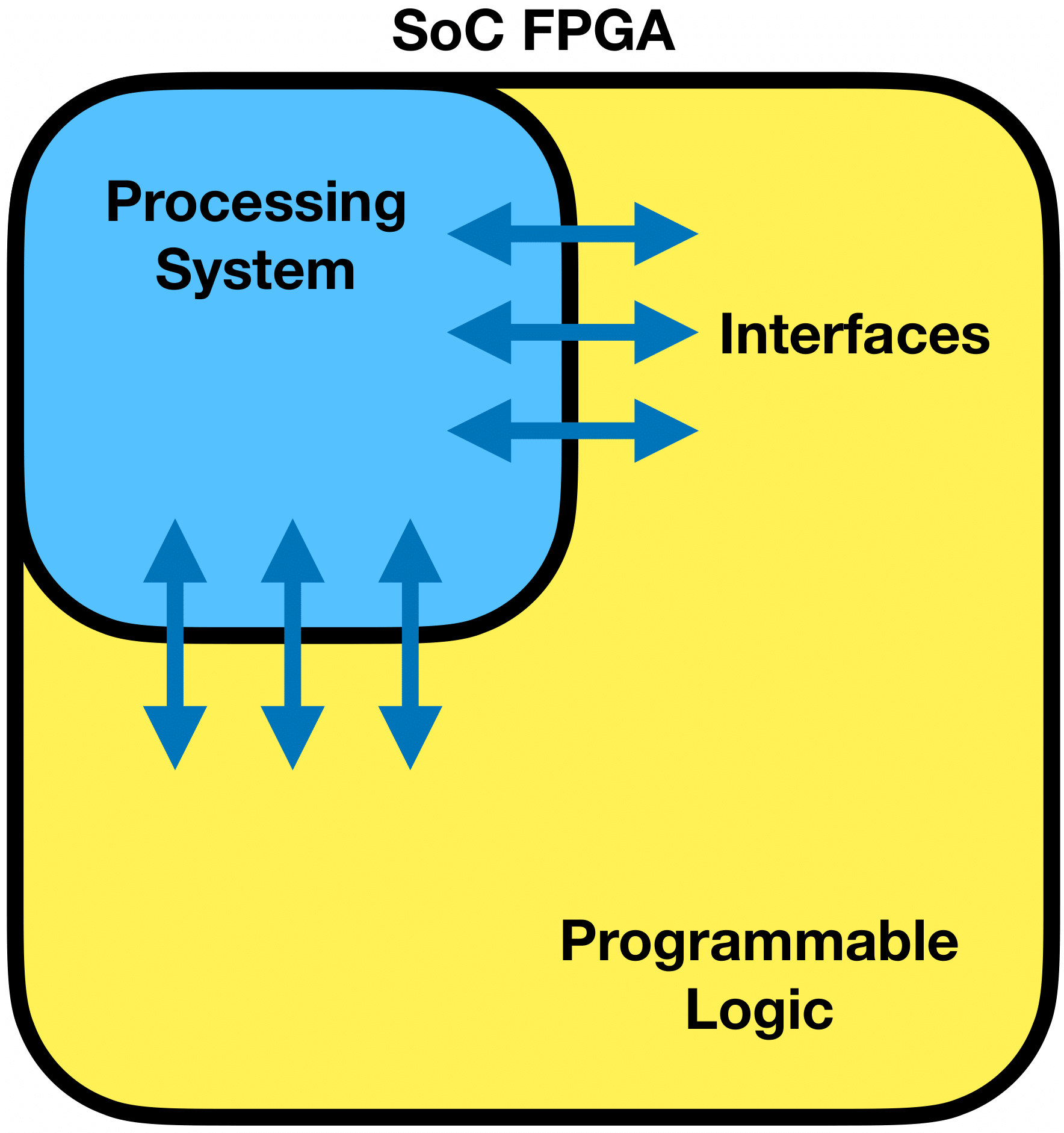
Figure 9: Block diagram illustration of a System on a Chip (SoC) FPGA, highlighting the division between the processing system and the programmable logic part, as well as the communication between them.
Development
In order to configure FPGAs, a developer needs to use a specialized computer language called Hardware Description Language (HDL). This type of language is used for describing the structure and behavior of electronic circuits, usually for ASICs and FPGAs. This design abstraction is known as Register-Transfer Level (RTL), modeling the digital logic circuit in terms of the flow of signals between the registers [Ref]. HDLs differ from normal programming languages because they describe concurrent hardware operations and timing behavior rather than sequential instruction execution. Because of this particularity, FPGA programming is notoriously difficult and comes with a high resource cost.
After the RTL description has been validated with test benches, the design is synthesized and the RTL description is translated to the gate-level description of the circuit. Finally, the design is laid out and routed on the FPGA.
High-Level Synthesis
In order to avoid the cost related to developing FPGAs, various tools have been designed to abstract out the complexity in configuring FPGAs. One particularly well-known tool is High-Level Synthesis (HLS) [Ref]. It is an automated process that takes an abstract high-level description, in languages such as C, C++ and MATLAB, of a digital system and produces the RTL architecture that realizes the given behavior. The code at the algorithmic level is analyzed, architecturally constrained, and scheduled for transcompilation into an RTL design in HDL, which is then typically synthesized to the gate level using a logic synthesis tool.
Conclusion
In this article, I introduced parallelism, briefly summarized the histories of GPUs and FPGAs, and presented the CUDA programming model. I also described the architecture of FPGAs and touched upon the nuances of their design. While CPU remains the strongest candidate for general-purpose, control-intensive, and sequential tasks, offering flexibility and ease of programming, they lack in ability to parallelize at large scale. GPUs on the other hand are well-suited for highly parallel, throughput-oriented tasks, particularly those with structured, data-parallel workloads. FPGAs provide customizable hardware-level parallelism with low latency and high energy efficiency, ideal for real-time and resource-constrained applications. However, their programming complexity remain significant barriers. This comparison is illustrated in Fig. 10. The choice between the different architectures presented depends on many factors, including performance, energy efficiency, flexibility and cost. Understanding the trade-offs between these architectures is crucial for designing optimized pipelines that meet specific requirements on throughput, latency or power consumption.
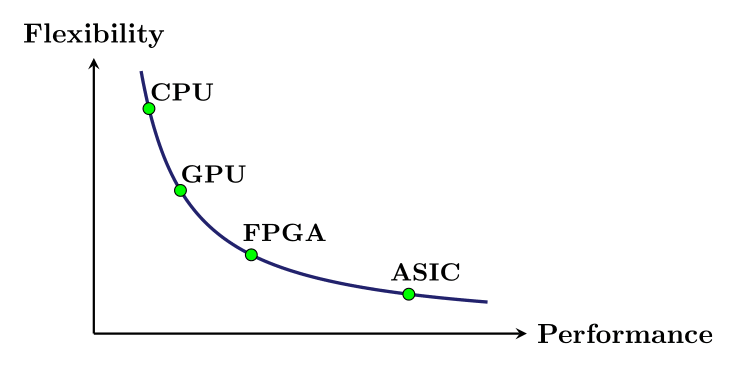
Figure 10: Illustration of a comparison of different processor architectures based on their flexibility and their performance potential.
This article is one of the chapters of my PhD thesis titled: “Real-Time Analysis of Unstructured Data with Machine Learning on Heterogeneous Architectures”. The full text can be found here: PhD Thesis. In the main results part of this work, GNNs were used to perform the task of track reconstruction, in the context of the Large Hadron Collider (LHC) at CERN.
HPC and parallelism have emerged as essential components of the processing infrastructure at LHC experiments at CERN. This development is largely driven by the need for Real-Time Analysis (RTA) at increasingly higher data rates. Meeting the stringent requirements for latency and throughput in such environments demands both specialized hardware and modern computing paradigms. Furthermore, specific types of hardware architectures are particularly interesting for exploiting parallelism in order to perform real-time analysis in high-energy physics, such as the GPU and FPGA architectures.
The background presented is crucial in understanding the computational aspects of the thesis work as well as the motivations behind it. HPC is particularly motivated by the need to perform RTA, which requires specific hardware and computing paradigms—such as parallel programming—in order to meet the strict latency and throughput constraints imposed by the extreme data rate environments at LHC experiments.
Comments